Every Extreme Ultraviolet (EUV) lithography scanner sold by ASML generates light the same way: a high-intensity carbon dioxide laser fires at tiny droplets of molten tin traveling at 100 meters per second, 50,000 times per second. The process, called Laser Produced Plasma (LPP), converts just 6% of the input energy into usable EUV photons. The other 94% is waste heat and debris.
Austin Lyons, a semiconductor analyst writing at Chipstrat, argues that this inefficiency is not merely an inconvenience but a structural cost crisis threatening the economics of advanced chipmaking. His piece on xLight, a Palo Alto startup building Free Electron Lasers for fabs, is both a physics primer and an investment thesis -- one that raises genuinely interesting questions about how the lithography supply chain might reorganize itself around a radically different light source.
"Stochastic print failures are far smaller, completely random and thus non-repeating, and come via a law of nature. The randomness is unavoidable. So how do we usually deal with randomness caused by the law of small numbers? We increase numbers. Just send more photons."
That quote, which Lyons pulls from Asianometry, captures the core dilemma. As chip features shrink, each pixel of photoresist covers fewer atoms, and statistical noise in photon absorption grows worse. The only remedy is a higher dose -- more photons per unit area. But higher dose means slower throughput unless the light source gets brighter.
Why LPP Is Hitting a Wall
Lyons lays out the math clearly. A Low-Numerical Aperture (NA) EUV tool is rated for about 220 wafers per hour, but that assumes a dose of 30 millijoules per square centimeter. High-NA tools, which print finer features, need 50 or more millijoules per square centimeter. The result is counterintuitive: the more advanced tool is actually slower.
"Every step to smaller features demands more dose, and more dose means fewer wafers per hour unless the light source gets brighter."
Current LPP sources produce about 500 watts of EUV power. ASML has shown a roadmap to 600-800 watts, and recently disclosed that its research team has unlocked 1,000 watts or more. But the dose treadmill keeps accelerating too.
Then there is the mirror problem. Tin debris fogs the collector mirrors -- a contamination layer just 1.2 nanometers thick cuts collector efficiency by 20%. Each mirror in the optical chain absorbs roughly 30% of the light that hits it. After the full series of reflections, less than 10% of source photons reach the wafer.
"Every scanner has its own dedicated LPP source. A fab running 15 EUV tools is operating 15 separate tin-burning light sources, each 6% efficient, each losing 90%+ to mirrors, each fighting its own debris."
That redundancy is staggering. Fifteen copies of a temperamental, debris-spewing, single-digit-efficiency light source, all running independently in the same building.
Free Electron Lasers as an Alternative
Lyons traces the history back to the 1980s, when the industry first attempted to use synchrotrons -- particle accelerators -- to generate EUV light. The approach failed because synchrotron radiation was too diffuse and non-directional. A Free Electron Laser (FEL) solves that problem through a fundamentally different mechanism.
"Instead of passively emitting radiation as electrons circle, an FEL actively amplifies coherent, directional light through a linear accelerator. Directional light! That distinction solves the problem that killed synchrotrons."
In an FEL, a linear accelerator shoots electrons to near light speed, then sends them through an undulator -- a chain of alternating magnets that forces the beam to wiggle. The wiggling electrons emit photons that interact with the beam itself, causing the electrons to self-organize into coherent bunches that amplify the light exponentially. No tin. No plasma. No debris.
Three properties make FELs attractive for lithography. The wavelength is tunable, meaning operators can dial the output to 13.5 nanometers for today's EUV scanners or go shorter for future nodes. Spent electrons can be looped back through the accelerator in reverse, recovering most of their kinetic energy. And without tin, the entire contamination problem disappears.
xLight's Bet: Photons as a Service
xLight, the company at the center of Lyons's analysis, is building an FEL designed to be backward compatible with ASML's existing scanner platforms. The swap is meant to be transparent from the scanner's perspective -- same angle, same wavelength, same intermediate focus point.
"xLight doesn't compete with ASML's scanners, but rather, replaces the light source. Unplug LPP, plug in xLight's FEL."
The numbers xLight is targeting are extraordinary. Their system is designed to generate 120 kilowatts of EUV power at the source. Current LPP sources produce just over 500 watts. That is a factor of roughly 240 times more power, though transmission losses through vacuum beamlines and grazing-incidence optics reduce what reaches any individual scanner to an estimated 2-4 kilowatts -- still several times more than LPP delivers today.
"Abundant light unlocks the full dose at full productivity. No more running $500M High-NA tools at a slower speed because you can't deliver enough photons."
The business model Lyons describes is unusual for semiconductor equipment: xLight would not sell hardware outright but instead sell light as a utility, a consumption-based service. One centralized FEL feeding an entire fleet of scanners, billed like electricity.
Where the Argument Gets Thin
Lyons makes a compelling case for the physics and the potential economics, but some of his strongest claims deserve scrutiny. The article acknowledges that no FEL has ever operated in a production semiconductor fab, yet frames the transition as primarily an engineering challenge rather than a scientific one. That framing understates the gap between laboratory demonstrations and 24/7 uptime in a cleanroom environment where any unplanned downtime costs millions per hour. Superconducting accelerator cavities, even with Fermilab's expertise, require cryogenic infrastructure and maintenance regimes that are wholly foreign to fab operations teams.
The suggestion that xLight could "arguably expand ASML's addressable market" is intriguing but speculative. ASML derives significant revenue from LPP light source servicing and upgrades. A third party capturing that revenue stream would represent a real threat, not just a complementary expansion, regardless of how many additional scanners fabs might buy.
The CHIPS Act Angle
xLight's prototype is being built at NY CREATES in Albany, New York, a semiconductor research and development hub where IBM runs a full 2-nanometer process flow and where Tokyo Electron, Applied Materials, and other major equipment companies maintain a presence. The prototype was accelerated by a $150 million letter of intent from the Commerce Department as part of the CHIPS Act research and development program.
"And they're not doing this in a garage. Their prototype is being built at NY CREATES in Albany, NY, a semiconductor R&D hub where IBM runs a full 2nm process flow."
That government backing matters. Building particle accelerators is expensive, and the CHIPS Act funding signals that the United States Department of Commerce sees FEL-based lithography as strategically relevant to domestic semiconductor manufacturing capability.
"xLight's prototype was accelerated by investment from the Commerce Department as part of the CHIPS Act R&D program."
Bottom Line
Lyons has written a technically rigorous piece that makes a clear case for why LPP light sources represent a growing bottleneck in advanced chipmaking. The physics are real: 6% conversion efficiency, compounding dose requirements, and tin debris contamination are genuine constraints, not marketing narratives from a startup. Whether xLight can translate laboratory FEL technology into a reliable, fab-grade utility operating at 120 kilowatts is an entirely different question -- one that will take years and billions of dollars to answer. For semiconductor investors and industry watchers, the article is essential reading on a technology that could reshape lithography economics. For skeptics, the paywalled second half reportedly covers the business model and adoption dynamics, which is where the hardest questions live.
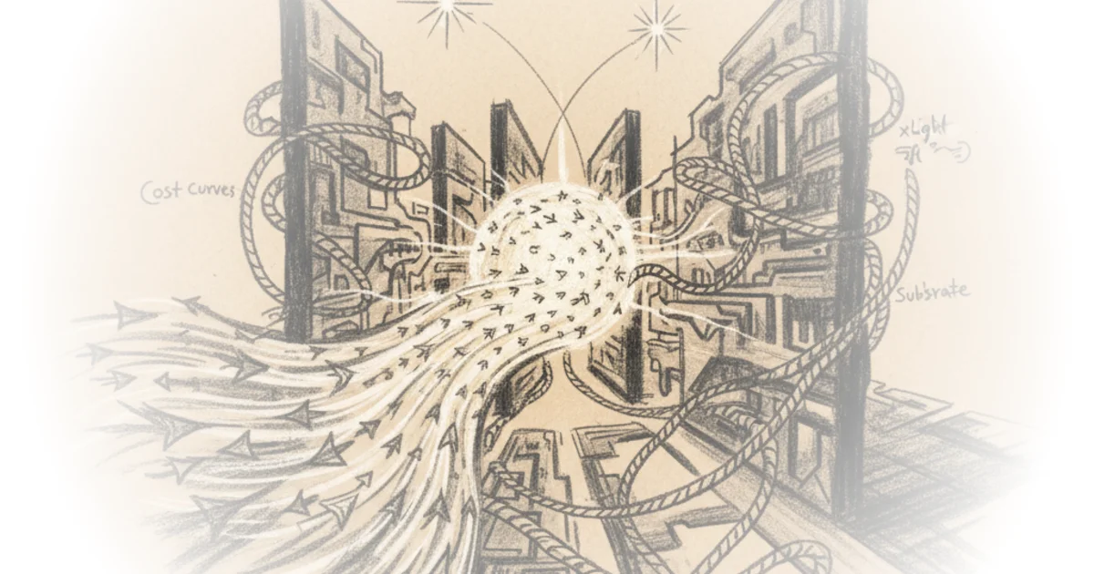
In January, I wrote about the worsening cost curve of EUV lithography and two startups trying to bend it:
I teased xLight and Substrate and promised deeper dives on both.
Today I’m delivering the first one on xLight. Now that we understand the broader economic problem the industry needs to solve, let’s dive into technical details and areas for improvement.
We’ll start with some fundamental limits of LPP EUV scanners.
The Photon Problem.
Every ASML EUV scanner generates its light the same way. It’s called Laser Produced Plasma, or LPP. It’s the “shoot tin droplets and hit ‘em each twice with a laser” light source magic trick. I’m assuming most readers are somewhat familiar, but if not here are great YouTubes references get you up to speed plus a short recap
How EUV’s light source LPP works: A high-intensity CO2 laser fires at tiny droplets of molten tin traveling at 100 meters per second, 50,000 times per second. Each droplet is actually hit twice: first a pre-pulse reshapes the 30-micrometer tin sphere into a concave sheet, then the main CO2 pulse vaporizes it into a dense plasma that emits 13.5nm EUV photons. These photons bounce off a series of collector mirrors, pass through a photomask, and expose the wafer below. As you can imagine, it took decades to get this concept to work at reliability and yield needed for scaled manufacturing. It’s freaking nuts that it works. That’s what I love about the semiconductor industry by the way, literally everywhere you look it’s just mind-blowing technology.
One interesting thing to note is that the industry actually first tried particle accelerators called synchrotrons to generate this high-energy, small-wavelength light. But at the time, synchrotrons didn’t have enough directional light. Next they tried xenon gas lasers, but that had a fundamental physics ceiling resulting in less than 1% conversion efficiency. Eventually the industry landed on tin back in 2002. Blasting tin particles into a plasma produces EUV light, but it has a debris problem (contaminating everything). That’s an engineering problem though (how to deal with this debris) but not a fundamental physics roadblock.
Fast forward 20 years and LPP with tin works. Hitting 50,000 falling tin droplets per second with a laser, twice each, 24/7. It’s genuinely an engineering marvel, should be discussed in freshman physics and engineering classes to get people excited about science