The semiconductor industry has long treated memory and storage as rigidly separate kingdoms: one for speed, the other for capacity. Chipstrat challenges this fundamental divide with a startling proposition—that flash memory, traditionally too slow for computation, can be engineered to rival high-end DRAM bandwidth simply by stacking it differently. This isn't just an incremental upgrade; it is a potential tectonic shift in how we build AI infrastructure, promising to slash the cost of running massive models without sacrificing performance.
The Architecture of Parallelism
The piece argues that High Bandwidth Flash (HBF) works not by making individual reads faster, but by making them massively parallel. "If you start the read it WAY before the accelerator needs the data, it could work," Chipstrat explains, reframing latency as a scheduling problem rather than a hardware limitation. By stacking 16 NAND dies vertically and connecting them with through-silicon vias (TSVs)—a technique familiar to those tracking the evolution of Through-Silicon Via technology—the system achieves a "width" that allows thousands of sub-arrays to read simultaneously.
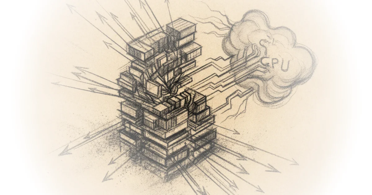
The result is a staggering leap in throughput. While conventional flash might deliver 14 GB/s, this new architecture delivers 1.6 TB/s, matching the bandwidth of HBM4 stacks. The article notes, "Roughly 100x the bandwidth, from packaging alone." This observation highlights a critical trend: the bottleneck is shifting from raw material properties to advanced packaging capabilities. Just as the industry moved from planar transistors to 3D stacking in logic chips, the memory hierarchy is now being redefined by how components are bonded together.
"HBF unlocks high bandwidth by stacking NAND dies to increase the 'width' or the parallelism... Any single read still takes thousands of nanoseconds, but thousands of reads can run in parallel."
Critics might note that this approach relies heavily on the assumption that AI workloads are predictable enough for prefetching. If a model's memory access pattern becomes too random or chaotic, the microsecond-level latency of flash could still cause significant stalls. However, the piece contends that inference decode is uniquely suited for this, as it often follows deterministic patterns.
The Economics of Scale
The economic implications are where HBF moves from technical curiosity to strategic necessity. Current AI models are becoming so large that they outstrip the capacity of standard High Bandwidth Memory (HBM). Chipstrat points out a grim reality for data center operators: "Bigger models mean more GPUs." Because HBM is co-packaged with the accelerator in fixed amounts, expanding memory requires adding entire expensive GPU units, along with the power and interconnect costs that accompany them.
HBF offers an escape from this escalation. With a single stack capable of holding 512 GB—roughly 10 times the capacity of current HBM4 configurations—the technology could allow massive models to reside on fewer chips. "A 70B parameter model... requires 140 GB just for weights," the article calculates, noting that a 1 trillion parameter model would need 2 TB. Storing this in HBF rather than HBM could reduce costs by an order of magnitude per gigabyte.
The piece emphasizes that while the raw NAND is cheap, the advanced packaging makes it expensive, yet still far more efficient than DRAM alternatives. "Sandisk claims a similar cost to an HBM stack despite 8-16x the capacity," Chipstrat reports, suggesting a future where edge devices or on-premise enterprises can run frontier models without needing a hyperscale data center.
"Nvidia is the certification gate; custom silicon moves first."
This dynamic introduces a new layer of complexity: supply chain control. The article notes that Sandisk has partnered with SK Hynix for the stacking, aiming to standardize the interface through an OCP effort. This mirrors historical shifts in memory markets where open standards eventually displaced proprietary bottlenecks, much like how DDR standards unified DRAM after earlier fragmentation.
A New Memory Hierarchy
The argument rests on a specific workload profile: inference decode versus training. "Inference decode fits this profile; training does not," the editors assert. Training requires constant, heavy writing to update weights—a task NAND flash cannot handle due to low write endurance. However, inference primarily reads static model weights, making it an ideal candidate for HBF.
The piece cites John Carmack's observation that "model inference can have a deterministic memory access pattern," validating the technical premise that random access isn't always required. This distinction is crucial; it means HBF doesn't replace DRAM entirely but carves out a new, high-capacity tier specifically for storing model weights.
"The argument for HBF is that inference decode is the perfect workload... if the accelerator knows what data it needs in advance, it can prefetch it and avoid waiting on any single slow read."
A counterargument worth considering is the power efficiency trade-off. The article admits HBF has worse bandwidth-per-watt than HBM4, roughly 2x higher power consumption for the same throughput. For energy-constrained edge devices or massive-scale deployments where every watt counts, this penalty could be significant. Yet, if the alternative is adding more GPUs to hold the model in DRAM, the net power savings might still favor HBF.
Bottom Line
Chipstrat's analysis provides a compelling roadmap for how the industry can solve the memory capacity crisis facing AI development. The strongest part of the argument is its clear distinction between inference and training workloads, demonstrating that flash's traditional weaknesses are irrelevant to the specific demands of model deployment. Its biggest vulnerability lies in the execution risk: standardizing a complex new packaging format across competing suppliers while maintaining performance guarantees is historically difficult. Watch for the first 2026 samples from Sandisk; if they deliver on the 1.6 TB/s bandwidth promise, the memory hierarchy will be rewritten within two years.