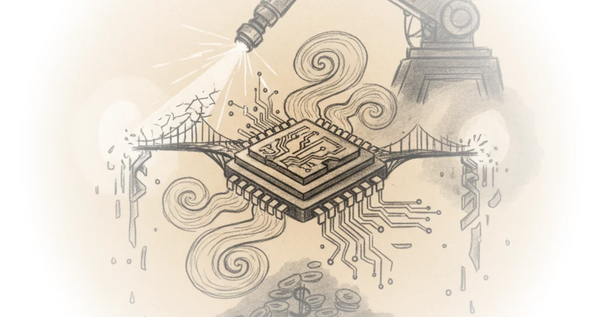
Asianometry dismantles the popular misconception that advanced semiconductor manufacturing is merely a matter of persistence, revealing instead that achieving 7-nanometer chips without Extreme Ultraviolet (EUV) lithography is a financial and engineering nightmare. While headlines often celebrate '7nm without EUV' as a triumph of ingenuity, this analysis exposes the brutal reality: it is a stopgap measure that sacrifices yield, efficiency, and design flexibility for the sake of market timing. For investors and policymakers tracking the global chip race, understanding the hidden costs of bypassing this technology is far more critical than the headline node number itself.
The Illusion of the Node Number
The piece begins by addressing the elephant in the room: the astronomical cost of EUV machines, which run around $150 million each. This price tag naturally leads to the question of necessity. Asianometry writes, "The answer is yes [you can do 7nm without EUV], but you won't want to and they probably won't work as well." This blunt assessment sets the stage for a deep dive into why the industry was forced to squeeze every drop of performance out of older Deep Ultraviolet (DUV) technology. The author traces the history from simple mercury lamps to the 193-nanometer Argon Fluoride lasers, noting that when EUV delivery targets slipped for a decade, the industry had to "squeeze more out of 193 over and over again."
This historical context is vital because it explains why the current semiconductor landscape is so fractured. The author argues that the industry's reliance on older tech wasn't a choice but a necessity born of delay. As Asianometry puts it, "The industry found itself needing to squeeze more out of 193 over and over again... until the Dutch cavalry arrives." This framing effectively shifts the narrative from one of technological stagnation to one of desperate adaptation. However, this adaptation came at a steep price, leading to a confusing marketing landscape where node names no longer reflect physical reality.
"The goal is for the end user to know that this node delivers better performing chips than the older generation. The smaller number still does this anyway."
Asianometry correctly identifies that the node naming convention has become a marketing abstraction rather than a physical measurement. By 2010, the literal half-pitch lengths had bottomed out, yet the industry continued to shrink the headline numbers to satisfy Moore's Law expectations. This disconnect means that a "7nm" chip from one manufacturer is not physically equivalent to a "7nm" chip from another. Critics might argue that this obfuscation harms consumer trust, but as the author notes, the industry prioritized the perception of progress over literal accuracy, a move that has complicated global supply chain analysis.
The Computational and Economic Trap of Multiple Patterning
The core of the argument lies in the mechanics of how chips are made without EUV. To achieve smaller features with older light sources, manufacturers must use "multiple patterning," a process of exposing the wafer multiple times with different masks to create a single, finer image. Asianometry explains that while double patterning was manageable, the industry soon had to adopt triple patterning and even self-aligned quadruple patterning to reach the 7nm equivalent. The complexity here is staggering. The author illustrates this with a stark computational reality: "For that same square four node structure triple patterning has 18 variations rather than just two with double."
This exponential explosion in design variations turns chip manufacturing into an NP-complete problem, where finding the optimal layout becomes computationally prohibitive. Asianometry writes, "This problem is not solvable in polynomial time... this is a massive slowdown and in the end the chip designers themselves had to be retrained to change their design tendencies." This is a crucial insight often missed in broader geopolitical discussions about chips; the bottleneck isn't just the machine, but the software and human expertise required to make it work. The economic burden is equally crushing. The author notes that triple patterning can make the lithography module "3.85 times higher" in cost compared to earlier nodes.
"Imagine trying to draw the rest of the f and owl but you can only use fix with parallel lines. This is extremely restrictive and makes for less efficient designs."
The analogy of drawing with fixed parallel lines perfectly captures the design constraints imposed by self-aligned quadruple patterning. It forces engineers to work within rigid boundaries, limiting innovation and efficiency. This section effectively argues that while it is possible to make 7nm chips without EUV, the process is so restrictive and expensive that it is commercially unviable for high-volume production. The author points to Intel's struggles as a case study, suggesting the company "tried to cross the n10 to n7 node gap without euv" and got caught in a yield trap, forcing them to use up to six exposures for a single feature.
The EUV Advantage and the Future of Co-Optimization
The narrative concludes by contrasting the struggle of multiple patterning with the relative elegance of EUV. Once the technology matured around 2016, the benefits were immediate. Asianometry writes, "With euv n7 features can be produced with up to 30 percent better cost efficiencies right off the bat even taking into account the euv machine's 150 million dollar price tag." This single statistic dismantles the argument that EUV is too expensive; the operational savings and yield improvements far outweigh the upfront capital cost. The author emphasizes that modern manufacturing is no longer just about shrinking transistors but about "design technology co-optimization," where the chip design and the manufacturing process are curated together like a "hipster's cafe."
This shift highlights a fundamental change in the industry: the days of simple scaling are over. The author warns readers against taking headlines at face value, stating, "Seven in one place isn't the same as seven in another. We shouldn't take headlines at face value. The devil is in the details." This is a powerful closing argument for a sophisticated audience, reminding them that the real story of the semiconductor industry is not in the marketing numbers but in the intricate, often invisible engineering trade-offs that determine who can actually produce the next generation of chips.
"The magic of human abstraction is that they take all these nuances and sweep it under the rug as a single number."
Bottom Line
Asianometry's analysis succeeds in demystifying the technical jargon surrounding semiconductor nodes, revealing that the ability to produce 7nm chips without EUV is a testament to engineering desperation rather than a viable long-term strategy. The strongest part of the argument is the detailed breakdown of the computational and economic penalties of multiple patterning, which effectively proves why the industry converged on EUV. The biggest vulnerability for any competitor attempting to bypass this technology is not just the lack of machines, but the insurmountable complexity of the design and manufacturing process itself. Readers should watch for how this technical reality shapes future trade policies, as the barrier to entry for advanced nodes is now defined by the ability to master EUV, not just the ambition to shrink transistors.