This piece cuts through the hype of AI chip wars to expose a quiet economic crisis: the packaging that holds these supercomputers together is becoming the most expensive part of the equation. Chipstrat argues that as chips grow beyond the physical limits of a single silicon wafer, the industry is hitting a "cost cliff" where traditional manufacturing methods simply cannot scale. For anyone tracking the future of artificial intelligence, the bottleneck isn't just the logic inside the chip—it's the glue holding it together.
The Reticle Wall
The article begins by grounding the reader in a hard physical constraint: the "reticle limit." This is the maximum area a lithography machine can expose in a single shot, roughly 858 square millimeters. Historically, chipmakers made processors faster by making them bigger, but that era has ended. "Blackwell broke through by stitching two reticle-sized compute dies together into a single GPU," Chipstrat notes, highlighting how the industry is now forced to stitch multiple pieces of silicon to create a single functional unit.
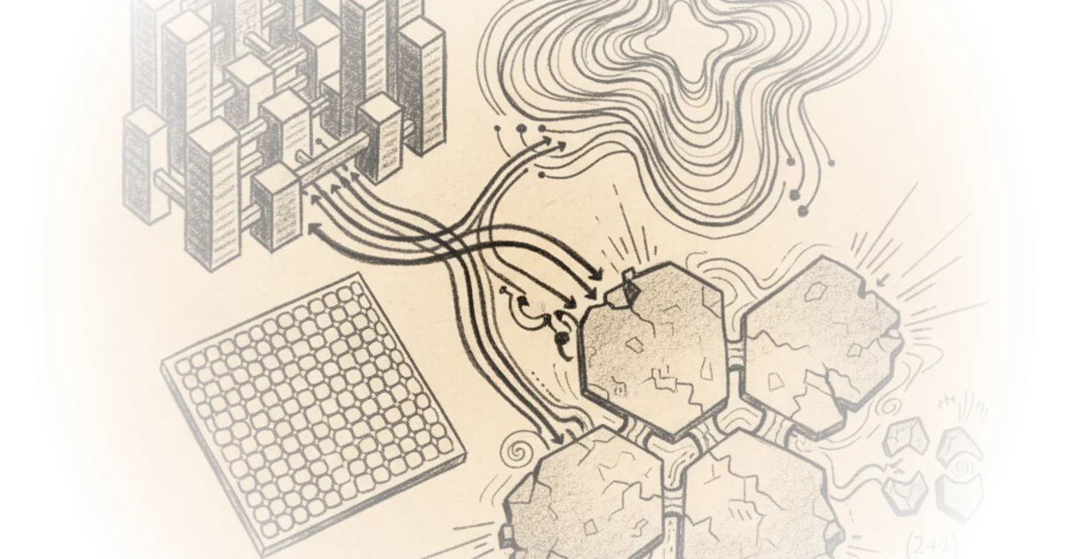
The piece explains that this shift has turned packaging from a back-end afterthought into the dominant cost variable in the bill of materials. "As AI accelerators keep getting bigger, the packaging itself is becoming the dominant cost variable in the bill of materials," the editors write. This is a crucial reframing. It suggests that the next breakthrough in AI performance won't necessarily come from a new transistor design, but from a new way of assembling the chip. The article draws a parallel to the evolution of Through-Silicon Vias (TSVs), noting that while TSVs enabled the vertical stacking of memory, the horizontal stitching of logic dies is now the new frontier.
"The ceiling on 'bigger' is the reticle limit... Once you cross that line... you need a way to physically connect multiple dies so they behave electrically like a single chip."
Critics might argue that focusing on packaging costs ignores the sheer revenue potential of these massive chips, but the piece makes a compelling case that if the assembly process fails or becomes too expensive, the economics of the entire AI boom could stall. The sheer scale of the problem is highlighted by rumors of warpage issues in Nvidia's upcoming Rubin Ultra, where a four-die package is struggling to stay flat.
The Battle of the Interposers
The commentary then dissects the two main contenders for solving this problem: TSMC's CoWoS (Chip-on-Wafer-on-Substrate) and Intel's EMIB (Embedded Multi-die Interconnect Bridge). The distinction is subtle but economically massive. TSMC's approach, particularly the CoWoS-L variant, uses a large silicon interposer—a passive layer of silicon that acts as a bridge between the compute dies and the substrate. "Think of it as a tiny circuit board made out of silicon," Chipstrat explains, noting that this interposer carries the signals but does no computing itself.
The article points out a fundamental inefficiency in this model: "The silicon wafer is being consumed for routing, not compute. That's expensive." Because the interposer is cut from a round 300mm wafer, but the package is rectangular, a significant amount of silicon is wasted at the edges. The piece cites Intel data suggesting that wafer utilization for these interposers is only about 60%, compared to 90% for rectangular panel-based processes.
In contrast, Intel's EMIB technology embeds tiny silicon bridges directly into the organic substrate, eliminating the need for a separate, massive interposer. "EMIB skips the interposer entirely," the piece argues. This architectural difference means Intel avoids three major cost centers: building the interposer, dicing it, and attaching it to the substrate. "Process steps eliminated: Interposer build, Interposer dicing, The interposer-to-substrate attach," Chipstrat lists, emphasizing that these are places where yield can drop and costs can skyrocket.
"At 14-reticle interposer sizes, you're approaching one interposer per wafer. One. Interposer. Per. Wafer. At that point the interposer absorbs the entire cost of the wafer."
This section is particularly strong because it moves beyond technical specs to the geometry of manufacturing. The article correctly identifies that as packages grow to 14 reticles or more, the round-wafer model becomes mathematically unsustainable. While TSMC is reportedly exploring "CoPoS" (Chip-on-Panel-on-Substrate) to move to rectangular panels, the piece notes that this is a workaround for a problem Intel's architecture solved by design.
The Yield Advantage
Beyond cost, the article makes a compelling case for yield. Bonding a massive, single-piece silicon interposer to a substrate is a thermal nightmare. Silicon and organic substrates expand at different rates when heated, leading to warpage and broken connections. "Warpage at that size is a yield-limiting problem," Chipstrat writes, directly linking this physical reality to the rumored struggles with the Rubin Ultra.
Intel's approach, by contrast, bonds smaller pieces individually. "EMIB attaches dies individually to the substrate. Each attach is small, locally thermally controlled, and decoupled from the others," the piece explains. This means that if one connection fails, the entire package doesn't have to be scrapped. The article suggests that this "small-piece bonding is inherently higher-yield than big-piece bonding," a claim that gains weight as package sizes continue to balloon.
The editors also touch on the future evolution of this technology, mentioning Intel's EMIB-T and EMIB-M variants which add vertical power flow and on-package capacitors. While the piece acknowledges that TSMC remains the dominant player, it frames the competition not as a battle of who can make the best chip, but who can assemble the largest chip without going bankrupt.
"The larger the package, the wider EMIB's margin gets. And packages keep getting larger every generation."
A counterargument worth considering is that TSMC's massive scale and established ecosystem might allow them to absorb these inefficiencies better than Intel can, regardless of the theoretical cost advantages of EMIB. The article hints at this by noting TSMC's ability to pivot to panel-level packaging, but it maintains that the geometric inefficiencies of the round-wafer model are a structural weakness that will only grow more pronounced.
Bottom Line
Chipstrat delivers a masterclass in connecting physical manufacturing constraints to economic reality, proving that the future of AI is as much about the substrate as the silicon. The strongest part of the argument is the geometric proof that round-wafer interposers cannot scale indefinitely without collapsing under their own cost. The biggest vulnerability lies in execution: while EMIB offers a superior theoretical model, Intel's track record in high-volume advanced packaging remains unproven compared to TSMC's dominance. The industry should watch closely to see if the physics of warpage and yield will force a rapid shift toward panel-based or bridge-embedded architectures in the next two years.